3D Chip Stacking Hits a Cost Wall Before It Hits the Market
For years the semiconductor industry has treated 3D integration as the obvious next step: instead of shrinking transistors further, you stack layers of chips on top of each other, shorten the distance signals travel, and get more performance out of the same footprint. The pitch is compelling, and the engineering has advanced fast. But a recent analysis from Chinese tech outlet TMTPost argues that the hardest problem is not whether chips can be stacked — it is whether stacking them makes financial sense.
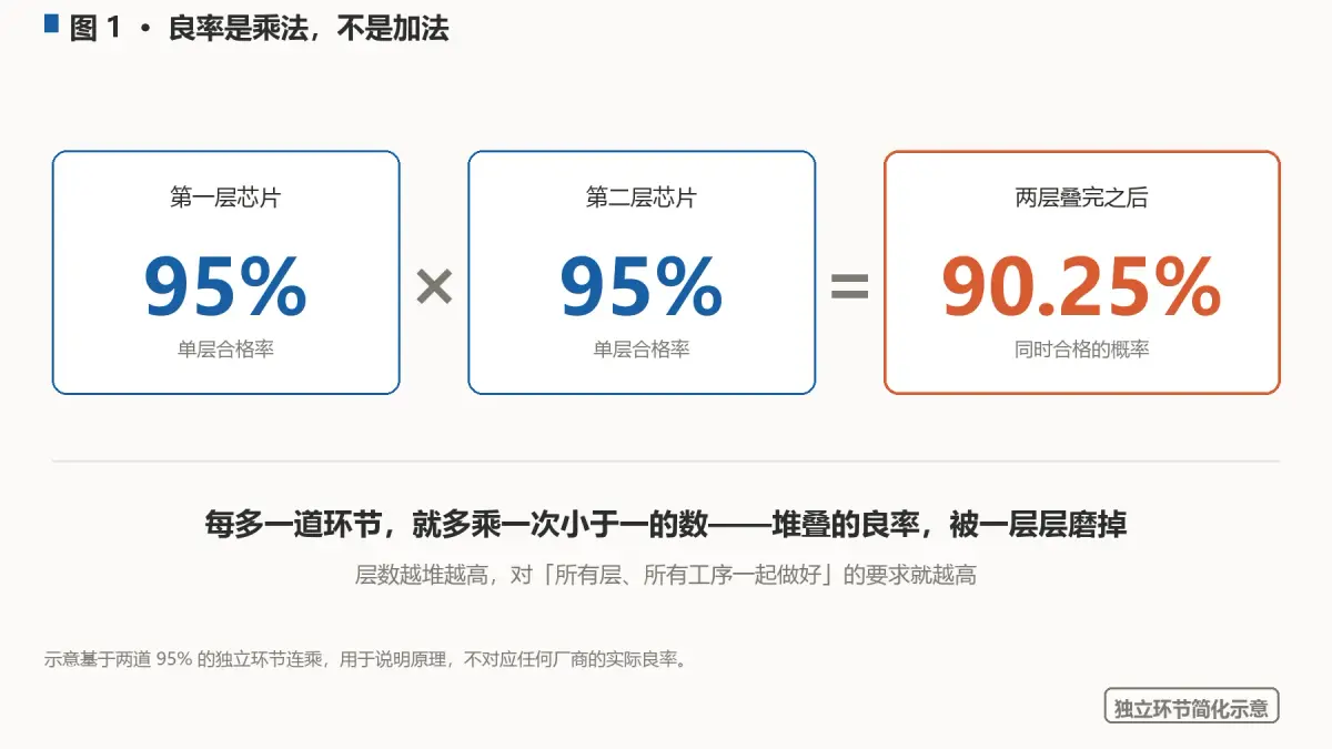
The technical achievement is real. Advanced bonding techniques now let manufacturers join wafers or dies with microscopic connections, and the precision keeps improving. Yet precision alone does not determine whether a product ships. What matters is yield: of all the stacks a factory starts, how many come out working. Every failed stack wastes not one chip but several, plus the costly steps used to bond and test them. When yields are low, the cost per good chip can balloon well beyond what customers will pay.
That arithmetic explains why 3D integration has arrived first in high-margin products. Memory makers have used vertical stacking for years because the value per chip is high enough to absorb imperfect yields. Logic chips are a harder sell. A processor that costs several times more to build only makes sense if it delivers a proportionate jump in performance or energy efficiency — and if buyers have no cheaper alternative.
There is also a testing problem. Defects can appear at any layer, and a fault buried deep inside a finished stack may only surface after the whole assembly is complete. Manufacturers are investing in ways to test intermediate layers before committing to the next one, which adds steps and time but can catch problems earlier. Each added step is another line on the cost sheet.
Equipment and materials suppliers sit in an awkward position. They benefit from every new stacking line that gets built, but their customers will only build those lines at scale once the economics work. That creates a chicken-and-egg problem familiar from earlier generations of packaging technology: volumes stay low, learning stays slow, and costs stay high until someone commits.
The most likely path forward is selective. Rather than stacking everything, chip designers will probably reserve 3D integration for the parts of a system where it pays — cache memory, high-bandwidth connections, specialized accelerators — and keep conventional designs elsewhere. Hybrid approaches let companies capture some of the benefit without betting an entire product line on unproven yields.
For China’s growing semiconductor sector, the question carries extra weight. Domestic firms have invested heavily in advanced packaging as a way to gain capability without relying on the most advanced lithography. That strategy only works if the resulting chips can be made cheaply enough to sell. Mastering bonding is one milestone; mastering the cost curve is the one that decides who survives.
None of this means 3D stacking is hype. It means the technology has entered the unglamorous phase where physics hands off to accounting. The winners will not be the teams that stack the highest, but the ones that figure out how to make every layer earn its keep.